The Benchmark Engineering Profile is an ongoing blog feature highlighting the engineering teams located around the world. Tune in every month to read the next installment in the series. This month features the engineers of Benchmark Lark Technology in Phoenix, Arizona. Next up: Benchmark Design Engineering in Tempe, Arizona.
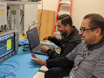
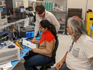
Benchmark Lark Technology is headquartered in Phoenix, Arizona, where it hosts Benchmark’s RF and High Speed Design Center of Innovation. Our engineering team works in a dedicated 30,000 square foot space that enables the vertical integration of system design, SMT, microelectronics assembly, and high density interconnect (HDI) substrate design and fabrication in one streamlined location. Lark is a world leader in RF circuits and components and circuit miniaturization.
Lark has been providing RF solutions for over 25 years and joined Benchmark in 2015. Since then, the talented engineers at Lark have been developing cutting edge solutions and have become an integral part of the Benchmark family. Our team at Lark is comprised of some of the most skilled and innovative engineers in the world.
We are Problem Solvers
The Design Center of Innovation and our engineering approach at Lark is focused first and foremost on solving complex problems. Our customers often bring us a problem— including problems they don’t believe have a solution—and our team works within the expanded design parameters made possible by our unique manufacturing processes to develop a solution. We solve RF and electronics miniaturization challenges that cannot be overcome using conventional design parameters. We are all problem solvers at heart and enjoy working collaboratively to resolve technical issues. This mindset is an integral part of our passion for our work, who we hire, and how we work with customers.
At Lark, we have extensive advanced communications, aerospace and defense design experience. We have designed everything from end-to-end radios and phased arrays to the smallest system-level components. Lark also has expertise in computing, complex industrial, and medical applications.
The variety of services and capabilities Lark provides to our customers includes cutting-edge PCB fabrication, miniaturization, receiver and transmitter design at the subsystem and system level, filter design, antenna design, PCB layout services and test services. Our advanced manufacturing techniques expand design options available and we can then produce our designs using our capabilities in microelectronics, SMT or even hybrid electronics.
 Our Process
RF design involves balancing many variables, so our process at Lark is simulation-centric to keep an eye on all of the factors. We use circuit/system simulators and 3-D electromagnetic modeling (EM) simulators to correlate lab measurements and accurately predict performance. This means we can handle a wide variety of projects with complex challenges, applying a custom approach and process to each customer we serve.
Our Work
We are proud to design and build solutions that overcome major technological barriers faced by our customers. Some recent examples include a Ka-Band SATCOM T/R module, mmWave multi-chain downconverter, and various mmWave phased array antennas.
One recent and particularly interesting design engagement was a 28-layer LCP high density interconnect (HDI) board with ball grid arrays (BGAs) of greater than 1,000 pins and trace, and spacing of less than 2 mils (50 microns). High signal pin count BGAs typically dictate printed circuit board (PCB) layer count; using conventional methods would have resulted in a layer count close to 50 layers. This is especially true when these application-specific integrated circuits (ASICs) consume a large portion of the PCB. Having the capability to route multiple fine lines and spaces between pads, having via-in-pads, and stacking micro-vias all help reduce the layer count. It is these capabilities that allow us to design a highly-dense, high-frequency, small form factor PCB for our customer.
Electronics Miniaturization
In addition to our work in RF, Lark offers unique electronic miniaturization capabilities. In all the industries we serve, customers are looking to add more capabilities to their devices without increasing the size of the product. Miniaturization is enabling products and technologies that were not previously possible.
The Lark manufacturing process uses a revolutionary additive/subtractive manufacturing technique capable of 10+ layer circuits with 25 micron lines and spaces. This creates a significant reduction in size, weight and power (SWaP) while supporting new electronics designs with improved performance.
We can help our customers achieve miniaturization at multiple levels. First, at the board level where we realize cutting-edge industry designs and second, at the system level where we can either design a solution ourselves or work with partners to achieve size reductions and performance that were previously unattainable. We work with a number of different substrates, including using RF-optimal materials like LCP while consulting with the customer to select the best materials for the specific application.
A Unique Approach
As is true with all Benchmark teams, our people are what is most important. Our engineers have a broad and diverse set of skills and experience in a wide range of industries. We do our best work when we’re faced with a complex challenge that forces us out of our comfort zone. It’s these challenges where we see the most innovative and disruptive solutions emerge.

Whether we’re developing high-frequency applications up to 110 GHz for secure military communication networks, improving the capability and form factor of IoT devices, or ushering in products compatible with the 5G era, Lark has the skills, experience and building blocks to help our customers innovate for the technology landscape of tomorrow.
Ready to find out how the Benchmark Lark Technology team can take on your tech challenges? Contact us.
