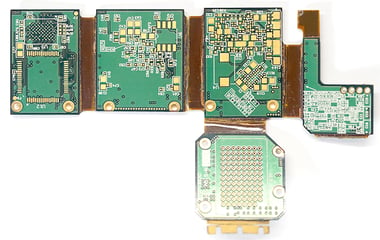
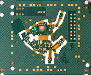
Today’s electronics-- whether it be a laptop or a missile control system-- are all partitioned in similar ways. Functions like power, RF signal processing, digital processing, etc. are often partitioned on separate boards that group the components required for that function. The way in which electronics are partitioned was standardized by a handful of market leaders back in the 1980s and smaller companies followed their lead until the entire electronics industry partitioned things similarly.
This was incredibly successful in proliferating electronics. With a finite set of components produced in massive quantities, the cost of each of those components went down. The ability to mix and match the standard components allowed new types of electronics to be developed quickly, spurring innovation. This was true of pagers and mobile phones, which could not have become affordable and widespread so quickly without standardized partitioning methods.
There was also a scientific basis for the way electronics were partitioned. For components built with materials and processes available at the time, it was easy for RF signals to interfere with digital processing and vice versa. Physically separating the two functions in space was the simplest way to avoid this kind of signal crosstalk.
 As market pressures drive more functionality into smaller devices, conventional partitioning has been the limiting factor. Even as components have packed more and more capability into ever-smaller packages, without reducing the total number of packages electronics designers can only get so far. Innovative smart phone OEMs spread their costs over volumes of 100s of millions and invested heavily in technology to begin breaking down some of these partitions; as a result, over the last 2-3 years mobile phones have begun to feature non-traditional partitioning.
Why is it now possible to do this without the system succumbing to crosstalk issues? In the past 40 years, materials and design parameters have evolved to provide new ways of avoiding crosstalk without physically separating the systems. New dielectrics and new processes for manufacturing with existing dielectrics such as Liquid Crystal Polymer (LCP) and polyimide provide integrity in very small lines and traces within the interconnect. In the example of modern smartphones, antennas and other circuits are now often produced in LCP or modified polyimide at a low layer count.
In aerospace, defense and medical devices, the need for re-partitioning to enable innovation may be even greater, but this has proven challenging without the production volume of consumer electronics to absorb the development costs. Producing boards in LCP or polyamide below 4-6 layers is no longer rare but may be insufficient to produce true systems-in-a-board that could eliminate partitioning.
 Standardized partitioning had its purpose and its moment, but the next revolution in electronics will be built on design flexibility. That’s why Benchmark invested in the materials and processes necessary to create boards with 1 mil lines and spaces in more than 10 layers with heterogeneous stackups. We combined this manufacturing capability with an industry- and application-agnostic design team. We saw that innovation was being stifled by the limitations of the manufacturing process and the impracticality of every defense, medical, communications, and compute OEM investing in developing these processes independently. Our solution is a Design Center of Innovation with design engineering and manufacturing co-located to overcome common challenges in design partitioning and high-frequency with materials that perform up to 110 GHz. We work with customers to choose the best material set for their use case, design high-performance, high-reliability solutions and ultimately scale production. With these technology solutions, we’re giving our customers new ways to partition that will enable an electronics revolution.
