Modern electronic circuit designs pack as much functionality and performance as possible into the smallest spaces, but this requires meeting challenging electrical and mechanical goals for printed circuit boards (PCBs). Fortunately, for years, Benchmark’s PCB design engineers have tracked the evolution of innovative, densely constructed high-frequency analog, high-speed-digital (HSD), and mixed-signal circuits, developing proven strategies for creating compact PCBs with impressive capabilities.
Balancing SWaP, Performance, and Reliability
The first step when designing a complex PCB is to consider the importance of basic circuit materials, packaging, shielding, and accessibility of test and measurement locations on a PCB. Starting with a customer’s electrical and mechanical specifications, developing creative—yet practical—PCBs to meet the most challenging sets of size, weight, power (SWaP), and performance goals is encouraged. Reliability and electromagnetic compatibility (EMC) must also be considered from the beginning of the process and not simply viewed as afterthoughts in the qualification phase. Engineers should optimize the design for the tests and validations required in the manufacturing phase, such as optical and electrical inspection, mechanical and electrical testing, and RF tests through millimeter wave frequencies. Electronic circuits perform an almost endless number of functions, from amplification to waveguide interconnections, and a PCB that can perform those functions with high efficiency and compact size will usually remain part of a product for a long time.
Given these considerations, designing and prototyping the PCB requires creativity, experience, and knowledge of realistic PCB layouts. Developing a practical PCB starts with a thoughtful review of the operating and performance specifications intended for that PCB. Numerous factors must be considered, including electrical, mechanical, and environmental constraints. For example, a microscopic surface-mount-technology (SMT) attenuator cannot be expected to process kilowatts of input power at any frequency without damaging it and the PCB. A PCB’s specifications should, therefore, be reviewed carefully for compatibility within a set of SWaP limits before attempting a fundamental circuit design with computer-aided design (CAD) software. High-density designs, for example, may require components mounted on both sides of a PCB.
Starting a Simulation
With the growing miniaturization and “densification” required for PCBs to pack more functionality into smaller boards, a newer PCB design may include bias power, digital, radio frequency (RF), microwave, and millimeter wave circuitry within a small area. Computer simulations with a CAD model of the PCB design and layout help calculate the interactions between subcircuits at the operating conditions of interest. These interactions are highly influenced by the physical and electrical characteristics of the PCB material, such as the dielectric constant (DC), the dissipation factor (DF), and the coefficient of thermal expansion (CTE) in the x, y, and z axes.
As high-speed-digital (HSD) circuits advance in performance, the characteristics of circuit materials become critical. These characteristics determine whether a PCB can meet its mechanical and electrical goals under various operating conditions, like fluctuating power and temperature. For example, the dielectric consistency of a circuit material can impact signal amplitude and phase consistency, and the rigidity or flexibility of a circuit material can affect its mechanical integration into an electronic housing. Other considerations in selecting a circuit material are cost availability and how either—or both—may affect the production of a PCB in large quantities. At the prototype stage, if a board material is not readily available or a board house is unfamiliar, yields can suffer, schedules can slip, and tolerances can be exceeded. At higher frequencies, tolerances can make or break a design for its production feasibility in large quantities.
The components mounted on those PCBs should be carefully selected, not just for minimum SWaP requirements, but to meet specified mechanical conditions, such as final PCB height to fit within a system space or required environmental conditions for temperature, shock, and vibration. The placement of components and supporting circuitry within a PCB also involves consideration of each component’s operating characteristics, such as heat tolerance, harmonics, electromagnetic (EM) fields, and how emissions might alter the performance of nearby components. Thermal emissions from a power amplifier could potentially disrupt the synchronization of nearby sensitive digital features, such as a digital signal processor (DSP).
Balancing SWaP, EMC, and Manufacturability
Components and structures often guide mechanical PCB layout without electrical connections, such as heat pipes running from higher-power components, structural features like fasteners and spacers, and general dimensional constraints on the housing. Additional structures (e.g., EM shielding for EMC) may also be necessary. Still, they add to the size and weight of a PCBA and can influence the positioning of components and the routing of transmission lines around them. Again, suitable CAD simulations can provide insights into the number and location of heat sinks, shielding, and other structures that help a PCB meet performance goals without exceeding SWaP limits.
Armed with the proper design files, a manufacturer can produce a hardware version of the design with its selected component inventory, circuit materials, and other essential features. For a circuit layout to be successful, however, careful attention must be given to the PCB fabricator and assembler’s manufacturability guidelines, especially for densely packed PCB layouts, which include handling and placement of components with many different sizes and weights. (Fig. 1 below)
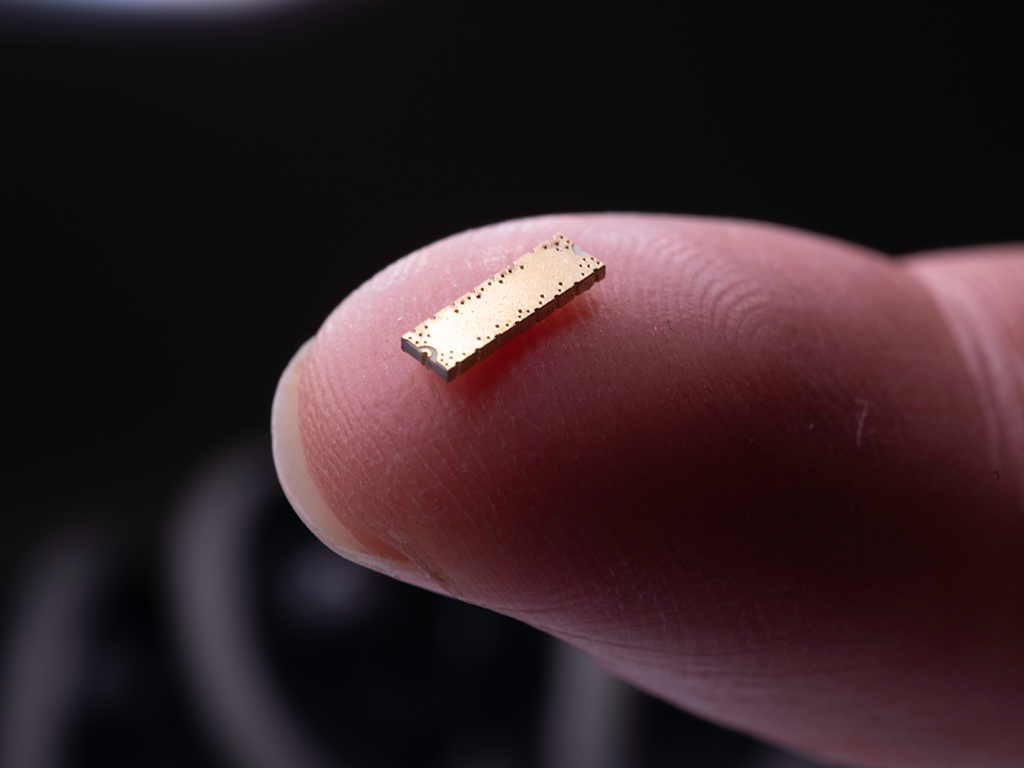
Figure 1:
Meeting modern reduced SWaP requirements for a PCB requires many microminiature components such as this SMT filter.
The addition of interconnections where needed is crucial for a successful manufacturing solution. Equally important is how a circuit layout facilitates characterization with modern automatic-test-equipment (ATE) systems, such as signal flow through the PCB and the ease of sampling these signals during testing.
Perusing the Prototype
Developing a prototype can provide helpful insights into the behavior and performance of a design. In all stages of the invention process—and throughout the development and manufacturing phases—close collaboration between the designer, fabricator, and assembler is essential. However, before engineers can test a prototype, they must inspect it for the safety and integrity of solder joints and signal interactions so that attempts to perform subsequent testing will be meaningful and cost-effective.
Although automated mechanical and optical inspection systems are not typically used for prototypes, such inspection systems can cover the minor details of a PCB’s assembly (including the attachment of integrated circuits and SMT components) and detect any physical anomalies that may result in a PCB’s operational or performance failure. A practical PCB layout will support different measurements at different test locations and make it possible to perform measurements under changing environmental conditions. A mixed-signal PCB, for example, may require access to test points for HSD signals, RF and microwave signals, millimeter wave signals, and power and control. If space concerns prohibit the integration of test points, a stand-alone interface board can be developed to offboard a subset of verification tests.
At the prototype phase, testability and rework capability are among the most critical elements of a design, but they should be given more consideration. To better understand the performance of a prototype PCB under changing environmental conditions, mechanical test gear can control the thermal conditions under which the PCB is tested and induce controlled levels of shock and vibration to emulate the operating conditions of many uses (e.g., airborne, space, naval, and terrestrial applications). (Fig. 2 below)
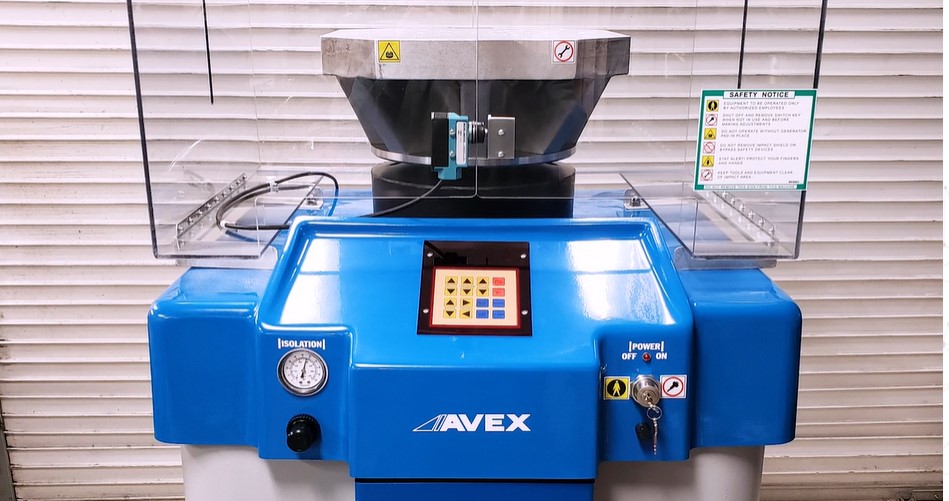
Figure 2:
Testing PCBs under altering shock and vibration conditions can prepare the PCB for challenging applications.
Providing PCB Support
Benchmark provides the many services required to assist designers in translating circuit concepts into practical, manufacturable PCBAs (including multilayer, mixed-signal PCBs) that meet demanding requirements for reduced SWaP. Benchmark often guides our customers on RF, microwave, millimeter wave, HSD, optical, and mixed-signal circuits using three-dimensional (3D) computer simulation capabilities to analyze the behavior of a circuit design over large ranges of operating conditions.
Benchmark helps you select effective layout designs, along with circuit materials, accessories, and components. Should any components from the original design become obsolete, we can help you source suitable replacements. To aid with characterizing a newly developed PCBA, Benchmark’s engineers help integrate test and measurement capabilities to create the most practical, reliable, and highest-performance prototype of a PCB design. Once the prototype is realized, our guidance includes complete characterization, test support, and access to in-house, production-level PCBA testing capabilities.
Connect with Benchmark to learn more about our PCB design and engineering capabilities.
