Optimizing size, weight, and power (SWaP) is the latest technology in electronics manufacturing. Be it medical, aerospace and defense, communications, or the consumer market, the need of the hour is a miniaturized product without any compromise of computing capability and efficiency.
Smaller Components, Bigger Challenges
Achieving acceptable results on the board fabrication end is not enough; it is equally important to be able to assemble the boards. The challenges in the assembly stage are inversely proportional to the size of the components used to populate the boards. The package sizes of passive components now are as small as 008004 (8 mils X 4 mils). At these sizes, components can get extremely difficult to rework and boards that cannot be reworked have a significant impact on the yield. Therefore, it is highly important for OEMs or contract manufacturers to have equipment and machinery that can handle such extreme cases.
Shrinking PCBs is a task when it comes to layout design as well. A keep out area is needed for all the components to be placed on the board. To accommodate the maximum number of components, PCB designers and layout engineers have to challenge the IPC specifications and manipulate the assembly keep outs of the components. Innovative layout techniques have to be developed to layout a high speed circuit while keeping the signal integrity intact.
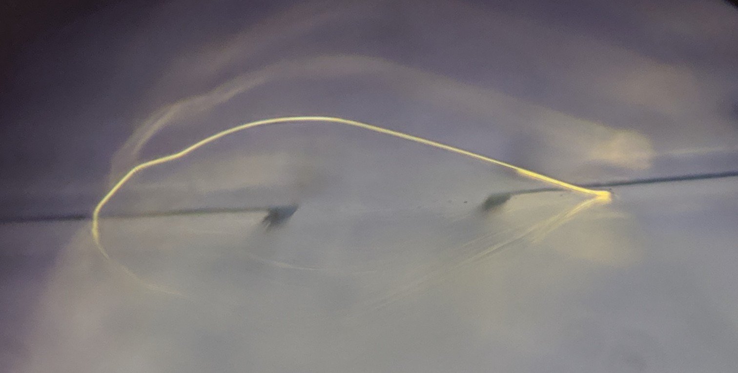 Photo: Ball bond using 1 mil gold wire
Design and Manufacturing Processes: Two Sides of One Coin
Designers have to consider the effect of micro-e processes on the design right from the beginning. For example, micro-e processes like wire bonding can have a significant impact on high frequency designs. It is very difficult to control volume production metrics like wirebond lengths, so it's necessary to account for the natural manufacturing variation by making the design more robust and less sensitive to the equipment tolerances or reasonable human error.
As a rule of thumb, a 5 mil long bond wire can add up to 5nH inductance in the circuit which in RF design accounts for a huge signal loss. Accounting for this loss in simulations gives the designers an understanding of how the circuit will behave, and they must depend on the manufacturing engineers to build the circuit as close as possible to the designed simulations. This is where Lark has a leading edge over other OEMs and contract manufacturers. With manufacturing and designing under one roof, assembled final products more closely match design specifications and simulations.
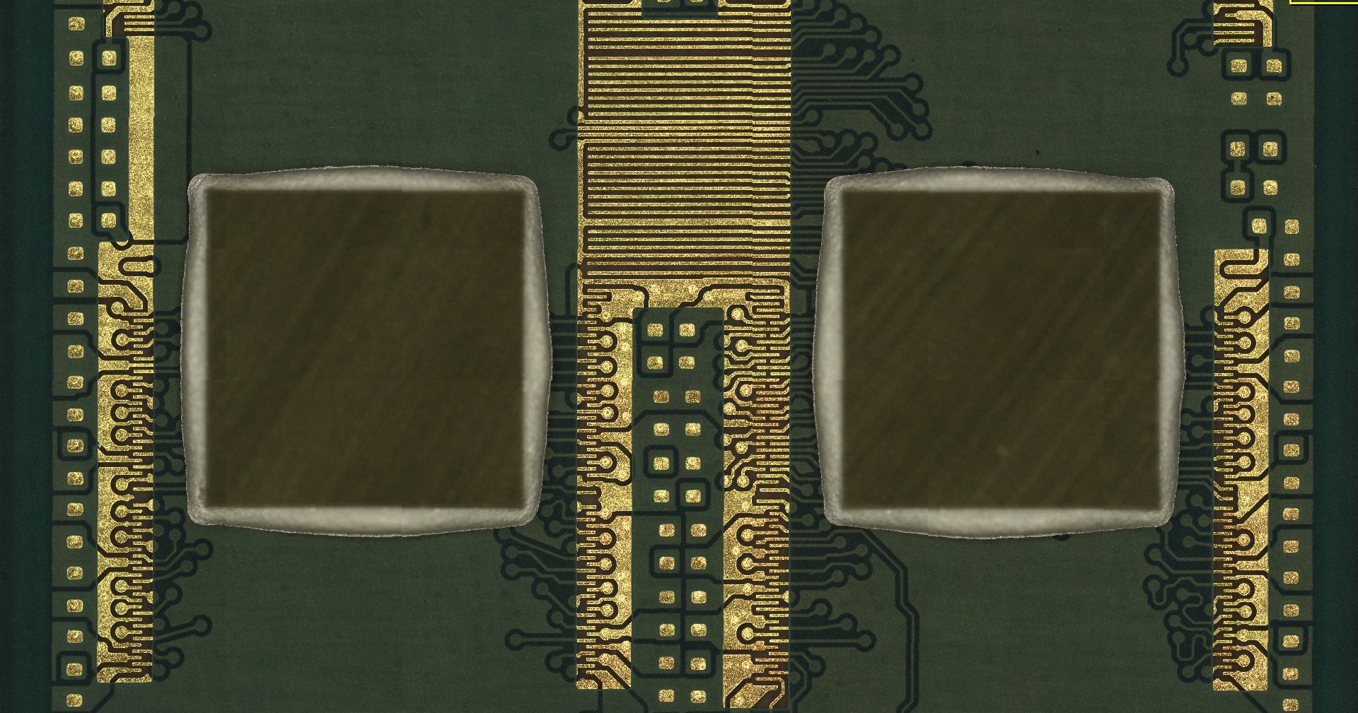
Photo: Die attached with adhesive
The Challenges of Hybrid Assemblies
Cutting edge, high power, and high frequency designs utilize various component packages like ball grid array (BGA), quad flat no-leads (QFN), bare die, and surface mount technology (SMT) all on one board. Traditionally, hybrid assemblies, i.e. boards with surface mount technology and micro-e technology such as wire bond, bare die, BGA, and QFN placement have always been a challenge due to the difficulty in packaging and handling bare die.
Benchmark Lark Technology solves this issue as it is a one-stop shop for hybrid assemblies. Lark has a state-of-the-art facility with equipment that supports SMT and an ISO 7 standard cleanroom for all micro-e related assemblies. On-site manufacturing and process engineers with a problem solving mindset are also a huge help when it comes to building a product with cutting edge technology.
With ever-shrinking boards, ultra-small components, and cutting edge technology, it is important for manufacturers to stay at the forefront in terms of equipment, skills, and manufacturing capability. Miniaturization is a tough mountain to climb, but we are confident that with our innovative design expertise, state-of-the-art facilities, and cutting edge manufacturing techniques, we are ready to meet the challenge.
Want to find out how Benchmark can help you overcome your manufacturability challenges in small electronics? Contact us!
